


- Product Description
-
Order data
Order Data Order No. CTSC-100 EM135, 4AI/1AQ×12BIT,,4input/1output,12BIT,Isolation CTS7 135-0KD10
- Technical Spec
-
Performance Parameters
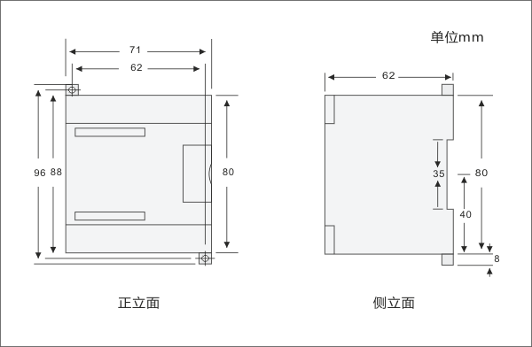
Specification EM135, 4 AI/1AQ×12BIT Physical Features Dimensions(W×H×D) 71.2×80×62mm Power Loss(dissipation) 2W Power Consumption From +5V(from I/O bus) 70 mA From L+ 48 mA L+ voltage range,class 2 or DC sensor supply 20.4~28.8V DC LED indicator24 VDC Power Supply Good
ON = no fault,
OFF = no 24 VDC powerAnalog Input Feature Number of analog input points 4 points Isolation(field side to logic circuit) Optical isolated: 500VAC, 1 minute Input type Differential Input Range Voltage(unipolar) 0-10V, 0-5V, 0-1V Voltage(bipolar) ±10V, ±5V, ±2.5V, ±1V Current 0~20 mA Data Range Unipolar,full-scale range 0~32000 Bipolar, full-scale range -32000~32000 Input Resolution Voltage(unipolar) 2.5 mV (0~10V)1.25 mV (0~5V)Voltage(bipolar) 2.5 mV (±5V)1.25 mV (±2.5V)Current 5μA (0~20mA) Analog to digital conversion time <300μs Analog input step response 100ms Common mode rejection 40dB,DC to 60Hz Common mode voltage Signal voltage + Common mode voltage < 12V Input Impedance ≥10MΩ Input filter attenuation -3db @ 3.1kHz Maximum input voltage 30V Maximum input current 30mA ADC resolution 15BIT Analog Output Features Number of analog output points 1 Signal range Voltage outputCurrent output±10V0~20mAResolution, full-scale Voltage outputCurrent output12BIT11BITData word format Voltage outputCurrent output-32000~+320000~32000Accuracy typical: ±0.5% of full scale; Worse: ±2% of full scale Setting time Voltage outputCurrent output100μs
2msMaximum drive@24VDC power Voltage outputCurrent output5000 ohm, minimum
500 ohm, maximumInput Calibration
The calibration adjustment will affect the instrumentation amplifier stage which follows the analog multiplexer. so the calibration affects all user input channels. Variations exist in the component parameters of each input circuit before the analog multiplexer will cause slight differences in the reading values between different channels connected to the same input signal even after calibration.If need to acquire the specifications contained in this data sheet, may be you need to enable analog input filters for all inputs of the module. Please select 64 or more samples to calculate the average value.To calibrate the input, please use the following steps.1. Turn off the power to the module, select the desired input range.2. Turn on the power to the CPU and module. Allow the module to stabilize for at least 15 minutes.3. Using a transmitter, a voltage source, or a current source, connect a zero value signal to one of the input channels.4. Read the value reported to the CPU from the input channel. Adjust the OFFSET potentiometer until the reading value is zero, or the desired digital data value.5. Connect a full-scale value signal to one of the input channels, read the value reported to the CPU. Adjust the GAIN potentiometer until the reading is 32000, or the desired digita data value.6. Repeat the OFFSET and GAIN calibration once more if requiredConfiguration
The calibration adjustment will affect the instrumentation amplifier stage which follows the analog multiplexer. so the calibration affects all user input channels. Variations exist in the component parameters of each input circuit before the analog multiplexer will cause slight differences in the reading values between different channels connected to the same input signal even after calibration.If need to acquire the specifications contained in this data sheet, may be you need to enable analog input filters for all inputs of the module. Please select 64 or more samples to calculate the average value.To calibrate the input, please use the following steps.1. Turn off the power to the module, select the desired input range.2. Turn on the power to the CPU and module. Allow the module to stabilize for at least 15 minutes.3. Using a transmitter, a voltage source, or a current source, connect a zero value signal to one of the input channels.4. Read the value reported to the CPU from the input channel. Adjust the OFFSET potentiometer until the reading value is zero, or the desired digital data value.5. Connect a full-scale value signal to one of the input channels, read the value reported to the CPU. Adjust the GAIN potentiometer until the reading is 32000, or the desired digita data value.6. Repeat the OFFSET and GAIN calibration once more if requiredTable 1 shows how to configure the EM 135 module using the configuration DIP switches. Switches 1 through 6 select the analog input range and resolution. All inputs are set to the same analog input range and format. Table 2 shows how to select for unipolar/bipolar (switch 6), gain (switches 4 and 5), and attenuation (switches 1, 2, and 3). In these tables, ON is closed, and OFF is openTable 1 EM 135 Configuration Switch Table to select Analog Input Range and Resolution
Unipolar Full-Scale Input Resolution SW1 SW2 SW3 SW4 SW5 SW6 OFF ON OFF OFF ON ON 0 to 1 V 250 uV ON OFF OFF OFF OFF ON 0 to 5 V 1.25 mV ON OFF OFF OFF OFF ON 0 to 20 mA 5 uA OFF ON OFF OFF OFF ON 0 to 10 V 2.5 mV Bipolar Full-Scale Input Resolution SW1 SW2 SW3 SW4 SW5 SW6 OFF OFF ON OFF ON OFF +1 V 500 uV ON OFF OFF OFF OFF OFF +2.5 V 1.25 mV OFF ON OFF OFF OFF OFF +5 V 2.5 mV OFF OFF ON OFF OFF OFF +10 V 5 mV Table 2 EM 135 Configuration Switch Table to select Unipolar/Bipolar, Gain, and Attenuation
EM 135 Switches Unipolar/Bipolar
SelectGain Select Attenuation
SelectSW1 SW2 SW3 SW4 SW5 SW6 ON Unipolar OFF Bipolar OFF OFF x1 OFF ON x10 ON OFF x100 ON ON invalid ON OFF OFF 0.8 OFF ON OFF 0.4 OFF OFF ON 0.2 Input Data Word Format

Note
12 bits readings of the analog-to-digital converter (ADC) are left-justified in the input data word format. The MSB is the sign bit: zero indicates a positive data word value. In unipolar format, the three trailing zeros cause the data word to be changed by a count of eight for each one-count change in the ADC value. In bipolar format, the four trailing zeros cause the data word to be changed by a count of sixteen for each one count change in the ADC value.
Output Data Word Format

The 12 bits readings of the digital-to-analog converter (DAC) are left-justified in the output data word format. The MSB is the sign bit: zero indicates a positive data word value. The four trailing zeros are truncated before being loaded into the DAC registers. These bits have no effect on the output signal value.
- Installation
-
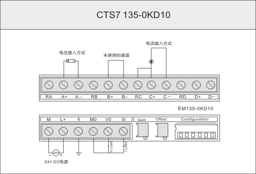
Wiring Diagram
Wiring Diagram